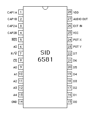
PIN CONFIGURATION
Picture 1. 6581 Pin Configuration
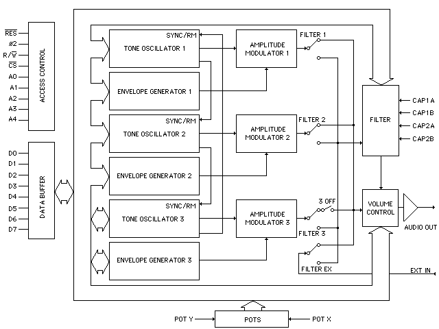
6581 BLOCK DIAGRAM
Picture 2. 6581 Block Diagram
SID PIN DESCRIPTION
CAP1A, CAP1B (Pins 1, 2)/ CAP2A, CAP2B (pins 3,4)
These pins are used to connect the two integrating capacitors requires by
the programmable filter. C1 connects between pins 1 and 2, C2 between pins
3 and 4. Both capacitors should be the same value. Normal operation of the
Filter over the audio range (approximately 30Hz- 12kHz) is accomplished
with a value of 2200 pF for C1 and C2. Polystyrene capacitors are preferred
and in complex polyphonic systems, where many SID chips must track each
other, matched capacitors are recommened.
The frequency range of the filter can be tailored to specific applications
by the chooice of capacitor values. For example, a low-cost game may not
require full high-frequency response. In thise case, larger values for C1
and C2 could be chosen to provide more control over the bass frequencies
of the filter. The maximum cutoff frequency of the filter is given by:
FCmax = 2.6E-5 / C
Where C is the capacitor value. The range of the Filter extends 9 octaves
below the maximum cutoff frequency.
[Transcriber's note: Allegedly, one of the designers should later have stated
that the above formula is wrong].
RES (Pin 5)
This TTL-level input is the reset control for SID. When brought low for
at least ten ø2 cycles, all internal registers are reset to zero
and the audio output is silenced. This pin is normally connected to the
reset line of the microprocessor or a power-on-clear circuit.
ø2 (Pin 6)
This TTL-level input is the master clock for SID. All oscillator frequencies
and envelope rates are referenced to this clock. ø2 also controls
data transfers between SID and the microprocessor. Data can only be transferred
when ø2 is high. Essentially, ø2 acts as a high-active chip
select as far as data transfers are concerned. This pin is normally connected
to the system clock, with a nominal operating frequency of 1.0 MHz.
R/W (Pin 7)
This TTL-level input controls the direction of data transfers between SID
and the microprocessor. If the chip select conditions have been met, a high
on this line allows the microprocessor to read data from the selected SID
register and a low allows the microprocessor to write data into the selected
SID register. This pin is normally connected to the system Read/Write line.
CS (Pin 8)
This TTL-level input is a low active chip select which controls data transfers
between SID and the microprocessor. CS must be low for any transfer. A read
from the selected SID register can only occur if CS is low, ø2 is
high and R/W is high.
A write to the selected SID register can only occur if CS is low, ø2
is high and R/W is low. This pin is normally connected to address decoding
circuitry, allowing SID to reside in the memory map of a system.
A0-A4 (Pins 9-13)
These TTL-level inputs are used to select one of the 29 SID registers. Although
enough addresses are provided to select 1 of 32 registers, the remaining
three register locations are not used. A write to any of theses three locations
is ignored and a read returns invalid data. These pins are normally connected
to the corresponding address lines of the microprocessor so that SID may
be addressed in the same manner as memory.
GND (Pin 14)
For best results, the ground line between SID and the power supply should
be separate from ground lines to other digital circuitry. This will minimize
digital noise at the audio output.
D0-D7 (Pins 15-22)
These bidirectional lines are used to transfer data between SID and the
microprocessor. They are TTL compatible in the input mode and capable of
driving 2 TTL loads in the output mode. The data buffers are usually in
the high-impedance off state. During a write operation, the data buffers
remain in the off (input) state and the microprocessor supplies data to
SID over theses lines. During a read operation, the data buffers turn on
and SID supplies data to the microprocessor over these lines. The pins are
normally connected to the corresponding data lines of the microprocessor.
POTX, POTY (Pins 24, 23)
These pins are inputs to the A/D converters used to digitize the position
of potentiometers. The conversion process is based on the time constant
of a capacitor tied from the POT pin to ground, charged by a potentiometer
tied from the POT pin to +5 volts. The component values are determined by:
R*C = 4.7E-4
Where R is the maximum resistance of the pot and C is the capacitor. The
larger the capacitor, the smaller the POT value jitter. The recommended
values for R and C are 470 kOhm and 1000 pF. Note that a separate pot and
cap are required for each POT pin.
Vcc (Pin 25)
As with the GND line, a separate +5 VDC line should be run between SID Vcc
and the power supply in order to minimize noise. A bypass capacitor should
be located close to the pin.
EXT IN (Pin 26)
This analog input allows external audio signals to be mixed with the audio
output of SID or processed through the filter. Typical sources include voice,
guitar, and organ. The input impedance of this pin is on the order of 100
kOhm. Any signal applied directly to the pin should ride at a DC level of
6 volts and should not exceed 3 volts p-p.
In order to prevent any interference caused by DC level differences, external
signals should be AC-coupled to EXT IN by an electrolytic capacitor in the
1-10 uF range. As the direct audio path (FILTEX = 0) has unity gain, EXT
IN can be used to mix outputs of many SID chips by daisy-chaining. The number
of chips that can be chained in this manner is determined by the amount
of noise and distortion allowable at the final output. Note that the output
volume control will affect not only the three SID voices, but also any external
inputs.
AUDIO OUT (Pin 27)
This open-source buffer is the final audio output of SID, comprised of the
three SID voices, the filter and any external input. The output level is
set by the output volume control and reaches a maximum of 2 volts p-p at
a DC level of 6 volts. A source resistor from AUDIO OUT to ground is required
for proper operation. The recommended resistance is 1 kOhm for a standard
output impedance.
As the output of SID rides at a 6-volt DC level, it should be AC-coupled
to any amplifier with an elctrolytic capacitor in the 1-10 uF range.
Vdd (Pin 28)
As with Vcc, a separate +12 VDC line should be run to SID Vdd and a bypass
capacitor should be used.
6581 SID CHARACTERISTICS
ABSOLUTE MAXIMUM RATINGS
Rating			Symbol	Value		Units
----------------------------------------------------------
Supply Voltage		Vdd	-0.3 to +17	VDC
Supply Voltage		Vcc	-0.3 to +7	VDC
Input Voltage (analog)	Vina	-0.3 to +17	VDC
Input Voltage (digital)	Vind	-0.3 to +7	VDC
Operating Temperature	Ta	0 to +70	degrees C
Storage Temperature	Tstg	-55 to +150	degress C
ELECTRICAL CHARACTERISTICS
(Vdd= 12 VDC + -5%, Vcc= 5 VDC +- 5%, Ta=0 to 70 degrees C)

CHARACTERISTIC		Symbol	Min	Typ	Max	Units
----------------------------------------------------------------
Input High Voltage	Vih	2	-	Vcc	VDC
Input Low Voltage	Vil	-0.3	-	0.8	VDC
(RES, ø2, R/W, CS, A0-A4,D0-D7)
------------------------------------------------------------
Input Leakage Current	Iin	-	-	2.5	uA
(RES, ø2, R/W, CS, A0-A4; Vin=0-5 VDC)

Three-State (Off)	Itsi	-	-	10	ua
(D0-D7; Vcc=max)
------------------------------------------------------------
Input Leakage Current
Vin= 0.4-2.4 VDC
------------------------------------------------------------
Output High Voltage	Voh	2.4	-	Vcc -0.7 VDC
(D0-D7; Vcc=min, I load= 200 ua)
------------------------------------------------------------
Output Low Voltage	Vol	GND	-	0.4	VDC
(D0-D7; Vcc=max, I load= 3.2 mA)
------------------------------------------------------------
Output High Current	Ioh	200	-	-	uA
(D0-D7; Sourcing, Voh= 2.4 VDC)
------------------------------------------------------------
Output Low Current	Iol	3.2	-	-	mA
(D0-D7; Sinking, Vol= 0.4 VDC)
------------------------------------------------------------
Input Capacitance	Cin	-	-	10	pF
(RES, ø2, R/W, CS, A0-A4, D0-D7)
------------------------------------------------------------
Pot Trigger Voltage	Vpot	-	Vcc/2	-	VDC
(POTX, POTY)
------------------------------------------------------------
Pot Sink Current	Ipot	500	-	-	uA
(POTX, POTY)
------------------------------------------------------------
Input Impedance		Rin	100	150	-	kOhm
(EXT IN)
------------------------------------------------------------
Audio Input Voltage	Vin	5.7	6	6.3	VDC
				-	0.5	3	VAC
(EXT IN)
------------------------------------------------------------
Audio Output Voltage	Vout	5.7	6	6.3	VDC
(AUDIO OUT; 1 kOhm, load, volume=max)
One Voice On:			0.4	0.5	0.6	VAC
All Voices On:			1.0	1.5	2.0	VAC
------------------------------------------------------------
Power Supply Current	Idd	-	20	25	mA
(Vdd)
------------------------------------------------------------
Power Supply Current	Icc	-	70	100	mA
(Vcc)
------------------------------------------------------------
Power Dissipation	Pd	-	600	1000	mW
(Total)
----------------------------------------------------------------
6581 SID TIMING
READ CYCLE
Picture 3. 6581 Read Timing
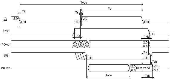
SYMBOL	NAME				MIN 	TYP 	MAX	UNITS
-------------------------------------------------------------------------
Tcyc	Clock Cycle Time		1	-	20	us

Tc	Clock High Pulse Widtch		450	500	10,000	ns

Tr, Tf	Clock Rise/Fall Time		-	-	25	ns

Trs	Read Set-Up Time		0	-	-	ns

Trh	Read Hold Time			0	-	-	ns

Tacc	Access Time			-	-	300	ns

Tah	Address Hold Time		10	-	-	ns

Tch	Chip Select Hold Time		0	-	-	ns

Tdh	Data Hold Time			20	-	-	ns
WRITE CYCLE
Picture 4. 6581 Write Timing
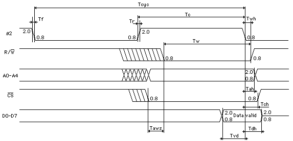
SYMBOL	NAME			     MIN	TYP	MAX	UNITS
-------------------------------------------------------------------------
Tcyc	Clock Cycle Time	     1	        -	20      us

Tw	Write Pulse Width	     300        -       -       ns

Twh	Write Hold Time		     0          -       -	ns

Taws	Address Set-up Time	     0       	-	-	ns

Tah	Address Hold Time	     10       	-	-	ns

Tch	Chip Select Hold Time	     0       	-	-	ns

Tvd	Valid Data		     80       	-	-	ns

Tdh	Data Hold Time		     10       	-	-	ns
